EMI/EMC design for medical devices protects the patient by making sure the device neither disturbs the equipment around it nor misreads, drops out or shuts down when that equipment disturbs it, through decisions taken at schematic and layout stage rather than at the test lab. That is why EMI/EMC design is a safety net for MedTech devices, not a certificate.
If you are specifying a medical device now and want it to pass EMC first time: ask your hardware team where the grounding strategy is written down, which interfaces carry filtering and protection at the board edge, when pre-compliance testing is scheduled and which edition of IEC 60601-1-2 the test plan cites. Those four answers tell you whether EMC is being designed or hoped for.
In medical device engineering, electromagnetic interference (EMI) and electromagnetic compatibility (EMC) are often misunderstood as certification requirements that appear late in development. EMI/EMC considerations are fundamental to device reliability and patient safety.
When electronic medical systems fail due to interference, the consequences are not just technical; they can be clinical. A monitoring device displaying inaccurate readings, a wearable losing signal integrity, or a therapy device experiencing communication disruption can directly impact patient outcomes.
That is why EMI/EMC readiness must be treated as a core principle of medical device hardware design, not a compliance checkbox at the end of development.
Why does EMI/EMC matter more in MedTech than in consumer electronics?
EMI/EMC matters more in MedTech because a medical device works in a room full of other emitters, imaging systems, infusion pumps, ventilators, wireless networks and phones, while itself emitting through switching regulators, radios, microcontrollers and high-speed interfaces. It must neither disturb those systems nor be disturbed by them, and a disturbance is a clinical event, not a glitch.
Medical devices operate in electrically complex environments. Hospitals and clinical settings are filled with electronic equipment: imaging systems, infusion pumps, ventilators, wireless networks, and mobile devices. Each of these can introduce electromagnetic disturbances.
At the same time, medical devices themselves generate electromagnetic emissions through switching regulators, wireless modules, microcontrollers, and high-speed digital interfaces.
The challenge is twofold:
- Devices must not emit interference that affects other systems.
- Devices must remain immune to external interference.
This balance defines electromagnetic compatibility.
In medical device hardware design, achieving this balance is essential for regulatory approval and safe clinical operation.
That two-way requirement is the subject of IEC 60601-1-2, edition 4.1, which covers both the device’s basic safety and essential performance in the presence of electromagnetic disturbances and the disturbances the device itself emits.
What does it cost to treat EMI/EMC too late in a medical device programme?
Treating EMI/EMC too late in a medical device programme costs a redesign cycle: PCB layout changes, shielding redesign, component replacement, filtering adjustments, enclosure modifications and repeated compliance testing, each of which moves the launch date. Designed in from the architecture, most of those risks never appear, and the lab visit confirms the design instead of discovering its faults.
Many engineering teams focus on functionality first and electromagnetic performance later. This approach often leads to expensive redesign cycles.
Late-stage EMI/EMC failures typically result in:
- PCB layout changes
- Shielding redesign
- Component replacement
- Filtering adjustments
- Enclosure modifications
- Repeated compliance testing
These changes are not only costly but also delay product timelines.
When EMI/EMC design is integrated early, most of these risks disappear. Preventive engineering is far more efficient than corrective engineering.
The cheapest place to find the cost is in the plan, before it is spent. On the programme for Pinetics’ own i.MX 8M Plus system-on-module and its carrier board, EMI/EMC test cycles are budgeted per hardware revision, so that a board re-spin does not silently skip re-testing. If the plan you are reviewing shows one EMC test at the end and no line for the revision that follows it, the second test is that redesign cycle, unbudgeted.
How should grounding and shielding be planned in a medical device?
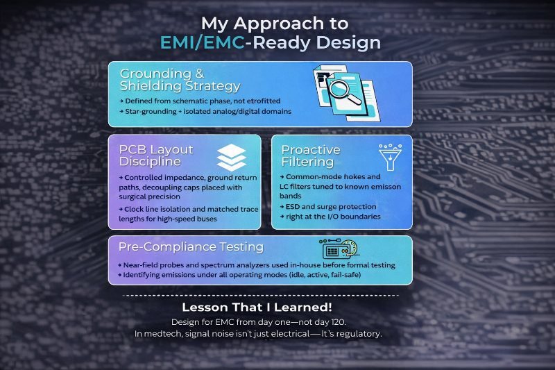
Grounding and shielding in a medical device are planned at schematic stage, not after layout: analog and digital grounds separated, star-ground configurations where they fit, ground loops minimised, return current paths defined and shielding decided with the enclosure. Sensitive analog front ends for ECG, EEG and bio signal acquisition are isolated from noisy digital circuits before a trace is drawn.
One of the most critical aspects of EMI/EMC performance is grounding architecture. Effective medical device hardware design defines grounding strategy during schematic design, not after PCB layout.
Common best practices include:
- Separating analog and digital grounds
- Implementing star-ground configurations
- Minimising ground loops
- Ensuring consistent return current paths
- Using shielding where necessary
Sensitive analog front ends, especially those used in ECG, EEG, or bio signal acquisition systems, require careful isolation from noisy digital circuits.
Shielding strategies must also be planned early to ensure enclosure design supports electromagnetic containment.
On a board with a mains side, the partition between mains and patient circuits is the line a review has to check rather than trust. Pinetics’ design review on a mains-powered patient-warming device caught the AC/DC isolation cutout misaligned in the PCB layout, and a copper-to-board-edge clearance that the chosen fabricator could not hold; both were fixed before fabrication. Neither would have shown up as an EMC failure first. The cutout would have shown up as a safety finding under IEC 60601-1, which is why grounding, isolation and EMC are reviewed as one drawing.
Which PCB layout practices keep a medical device EMC compliant?
The PCB layout practices that keep a medical device EMC compliant are continuous ground planes, decoupling at the IC power pins, controlled impedance on high-speed traces, minimal power loop areas, isolated clock lines and managed return current flow. USB, SPI and display buses need controlled routing because their fast edges radiate. Ask to see all six in the layout review.
PCB layout plays a decisive role in EMI/EMC performance. Even well-designed schematics can fail compliance testing if layout discipline is ignored.
Critical layout practices include:
- Maintaining continuous ground planes
- Placing decoupling capacitors close to IC power pins
- Controlling impedance on high-speed traces
- Minimising loop areas in power paths
- Isolating clock lines
- Managing the return current flow
In medical device hardware design, layout is not just mechanical placement; it is electromagnetic engineering.
High-speed interfaces such as USB, SPI, and display buses require controlled routing to prevent radiated emissions and signal-integrity issues.
Six PCB layout practices for a medical device, what each controls and the stage at which it is decided
| Layout practice | What it controls | Decided at |
|---|---|---|
| Continuous ground plane | Return path, loop area, radiated emissions | Stack-up, before layout |
| Decoupling at IC power pins | Supply noise, high-frequency current loops | Schematic and placement |
| Controlled impedance traces | Reflections and emissions on high-speed lines | Stack-up and routing |
| Minimal power loop area | Magnetic field emission from power paths | Placement |
| Isolated clock lines | Harmonic emissions coupling into neighbours | Routing |
| Managed return current | Ground bounce, common-mode noise | Stack-up and routing |
Ground plane continuity, controlled impedance and return current management are all settled in the stack-up, before the first component is placed. That is the reviewer’s shortcut: if the stack-up has not been agreed, the layout review has not started, however finished the board looks on screen.
How do you filter and protect a medical device's interfaces against EMI?
You filter and protect a medical device’s interfaces by treating every connector as a door: common-mode chokes on communication lines, LC filters on power inputs, transient voltage suppressors, ESD protection and ferrite beads on supply rails, all placed at the I/O boundary so a disturbance is contained before it reaches sensitive circuitry. Most of those parts cut emissions too.
External interfaces are common entry points for electromagnetic disturbances. Proactive filtering reduces both emissions and susceptibility.
Typical techniques include:
- Common-mode chokes on communication lines
- LC filters on power inputs
- Transient voltage suppression devices
- ESD protection circuits
- Ferrite beads on supply rails
Placing protection components directly at I/O boundaries ensures disturbances are contained before reaching sensitive circuitry.
This strategy improves device robustness and simplifies compliance testing.
The immunity half of that list is what the test lab will exercise directly: IEC 61000-4-2 is the electrostatic discharge test the ESD protection has to survive, and IEC 61000-4-4 and IEC 61000-4-5 are the fast transient and surge tests the suppression devices are chosen against. Ask which points on your device a patient or a clinician can touch; those are where the ESD test goes.
How do you manage power supply noise in a medical device?
You manage power supply noise in a medical device by choosing the switching frequency deliberately, grounding the regulators properly, filtering input and output, shielding high-current loops and minimising trace inductance, because the switching supply is usually the largest emitter on the board. Ask where its return current flows before it reaches the sensing front end.
Switching power supplies are often the largest source of electromagnetic emissions in medical devices.
Effective medical device hardware design must address:
- Switching frequency selection
- Proper grounding of regulators
- Input and output filtering
- Shielding of high-current loops
- Minimising trace inductance
Power supply layout requires careful attention to current paths and component placement.
Noise generated in the power domain can easily propagate into signal acquisition circuits if isolation is not maintained.
Typical switching frequencies and their harmonics fall inside the band CISPR 11 covers, 9 kHz to 400 GHz, which is why the switching frequency is a compliance decision and not only a thermal one.
Why does pre-compliance testing save time on a medical device?
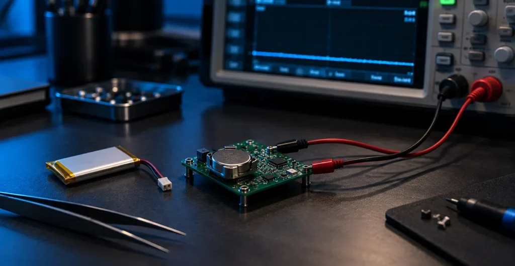
Pre-compliance testing saves time on a medical device because it finds emissions and susceptibility on the bench, with near-field probes, spectrum analysers, conducted emission set-ups and immunity tools, while the board can still be changed cheaply. Testing in every operating mode, idle, active, transmitting and in fault states, makes the formal test confirmation rather than discovery.
Pre-compliance testing is one of the most valuable practices in EMI/EMC engineering.
Instead of waiting for formal certification testing, teams can use:
- Near-field probes
- Spectrum analysers
- Conducted emission test setups
- Immunity testing tools
These allow engineers to identify emissions early and correct them before final validation.
Testing devices in multiple operating modes, idle, active, wireless transmission, and fault states, provides a realistic view of electromagnetic performance. This approach dramatically reduces certification risk.
Pre-compliance on the bench does not replace the accredited lab; it makes the lab visit a booked event rather than a gamble. Pinetics takes client hardware to an accredited third-party lab for EMI/EMC testing as a planned project task, with the components kitted for it in advance, so the test is a scheduled gate rather than an afterthought. Where that gate sits in a programme, between prototype bring-up and design transfer, is set out on our page on how a hardware and firmware programme runs from architecture to design transfer.
How does electromagnetic interference affect patient safety?
Electromagnetic interference affects patient safety by corrupting what a medical device senses and says: noise distorts bio signal acquisition, interference disrupts wireless telemetry, voltage spikes damage components and unstable communication interrupts therapy delivery. Each is a safety event, so a medical device is designed to stay stable in a noisy electromagnetic environment, not to work in a quiet one.
Electromagnetic interference can affect sensor accuracy, communication reliability, and the operation of control systems.
For example:
- Noise can distort bio signal acquisition
- Interference can disrupt wireless telemetry
- Voltage spikes can damage sensitive components
- Unstable communication can interrupt therapy delivery
In medical environments, these risks translate directly into safety concerns.
This is why EMI/EMC standards for medical devices are more stringent than those for consumer electronics. Engineering teams must design systems that remain stable even in noisy electromagnetic environments.
That is what the radiated immunity test is for: IEC 61000-4-3 defines the test method for immunity to a radiated radio-frequency electromagnetic field.
Which standards govern EMC testing for medical devices?
EMC testing for medical devices is governed by IEC 60601-1-2, the collateral standard to IEC 60601-1 for electromagnetic disturbances, which sets emission and immunity requirements for medical electrical equipment and systems. The tests themselves are defined by basic EMC standards: CISPR 11 for radio-frequency emissions and the IEC 61000-4 series for electrostatic discharge, radiated field, fast transient and surge immunity.
Medical device regulations require compliance with international EMC standards, including IEC 60601-1-2.
These standards evaluate:
- Radiated emissions
- Conducted emissions
- Electrostatic discharge immunity
- Radiated immunity
- Electrical fast transients
- Surge immunity
Passing these tests requires deliberate design choices, not last-minute fixes.
When EMI/EMC planning is integrated into medical device hardware design, regulatory approval becomes smoother and more predictable.
Six EMC tests for a medical device, the standard that defines each test method and where to find it
| EMC test | Standard defining the method | Source |
|---|---|---|
| Radiated emissions | CISPR 11:2024, RF disturbance limits, 9 kHz to 400 GHz | CISPR 11 page |
| Conducted emissions | CISPR 11:2024, the same document | CISPR 11 page |
| Electrostatic discharge immunity | IEC 61000-4-2:2025 | IEC 61000-4-2 page |
| Radiated immunity | IEC 61000-4-3:2020 | IEC 61000-4-3 page |
| Electrical fast transients | IEC 61000-4-4:2012 | IEC 61000-4-4 page |
| Surge immunity | IEC 61000-4-5:2014+AMD1:2017 | IEC 61000-4-5 page |
IEC 60601-1-2:2014+AMD1:2020, edition 4.1, “applies to the basic safety and essential performance” of medical electrical equipment “in the presence of electromagnetic disturbances” and to the disturbances the equipment itself emits; the IEC 60601-1 base standard is where basic safety and essential performance are defined. Pinetics is not an accredited test laboratory and holds no certification of its own; it designs to these standards inside the customer’s quality system, and the test report that goes into the customer’s design records comes from the accredited lab.
How do you design a medical device for EMC reliability, not just compliance?
You design a medical device for EMC reliability rather than compliance by asking where it will actually be used, hospitals, ambulances, homes, rural clinics and industrial medical settings, and designing for the noisiest of them rather than for the test chamber. A certificate proves the device passed a defined test once; reliability means it keeps working where interference is undefined.
The ultimate goal of EMI/EMC design is not certification; it is reliability.
Devices must perform consistently across:
- Hospitals
- Ambulances
- Home-care environments
- Rural clinics
- Industrial medical settings
Each environment presents different electromagnetic challenges.
Engineering for EMC resilience ensures devices remain dependable regardless of where they are used.
The home is the environment the standards single out. IEC 60601-1-11 defines the home healthcare environment as “the dwelling place in which a patient lives; other places where patients are present both indoors and outdoors, excluding professional healthcare facility environments where operators with medical training are continually available when patients are present”. In other words, no medically trained operator is continually available to notice a device misbehaving. Our post on why embedded systems fail in field conditions covers what field conditions do to embedded electronics more generally and how to design against them.
Why do medical devices fail EMC testing?
Medical devices fail EMC testing because electromagnetic behaviour was left to the test rather than decided in the architecture: grounding strategy defined late, PCB layout discipline relaxed, analog and digital systems not isolated, external interfaces unfiltered and no pre-compliance testing before the lab. If none of those five is written down for your device, the test date is the risk.
Across multiple medical device programmes, one lesson stands out clearly: EMI/EMC success begins with architecture, not testing.
The most successful designs:
- Define grounding strategy early
- Maintain strict PCB layout discipline
- Isolate analog and digital systems
- Filter external interfaces
- Perform pre-compliance testing
- Consider electromagnetic behaviour during system architecture
When these practices are followed, compliance testing becomes confirmation rather than discovery.
Every one of those choices is made before the lab books a slot to test the device against IEC 60601-1-2, and most of them before the board goes to fabrication.
What does EMI/EMC design look like when it is done correctly?
EMI/EMC design done correctly is invisible: the medical device reads, transmits and delivers therapy the same way in a crowded ward as on the bench, passes IEC 60601-1-2 testing at the first attempt and never appears in a redesign budget. Getting there takes deliberate planning at every stage, from the first schematic’s grounding strategy to the last revision’s test plan.
EMI/EMC engineering is often invisible when done correctly. Devices simply work reliably, safely, and predictably. But achieving that reliability requires deliberate planning throughout development.
Pinetics integrates EMI/EMC readiness into every stage of medical device hardware design, from the grounding and isolation decisions on the schematic, through layout review and pre-compliance on the bench, to the accredited third-party lab test booked as a planned project task, so that the device meets regulatory requirements while keeping its signal integrity and operational stability where it is used. That work rests on 100,000+ engineering hours and a leadership team with 20+ years of experience, and it runs inside the customer’s quality system rather than under a certification of our own. By designing electromagnetic compatibility from the start, we help medical innovators avoid costly redesigns and deliver products that perform safely in real-world environments; if your device has a test date and no written grounding strategy, that is the conversation to have first.
In MedTech, EMI/EMC design is more than an engineering discipline. It is a safety net that protects patients, clinicians, and the technology they depend on.
Sanjay Barewar, Director, Co-Founder and Global Chief Delivery Officer, Pinetics. 22+ years in electronic product development. BE Electrical, Pune University. LinkedIn